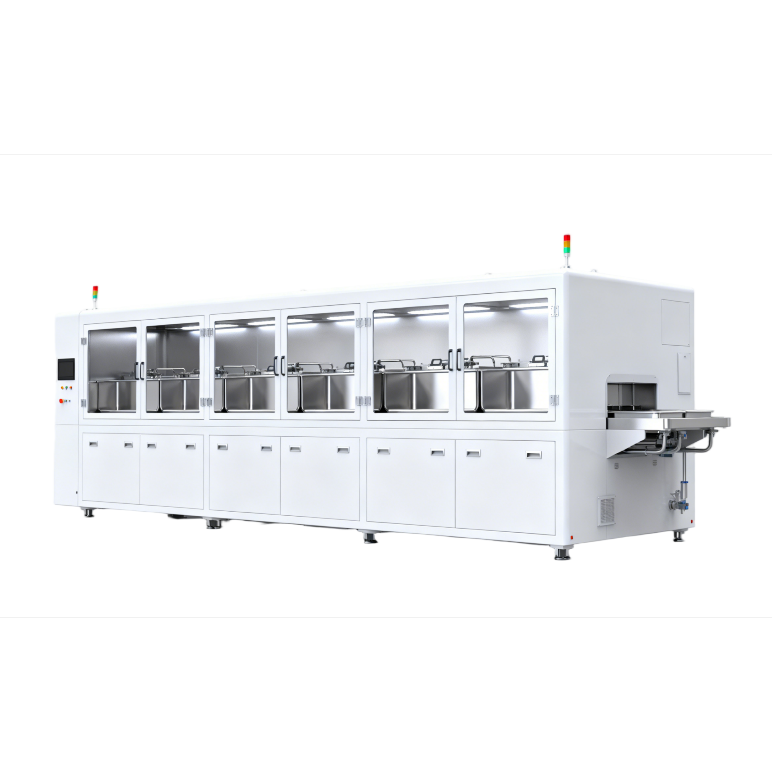
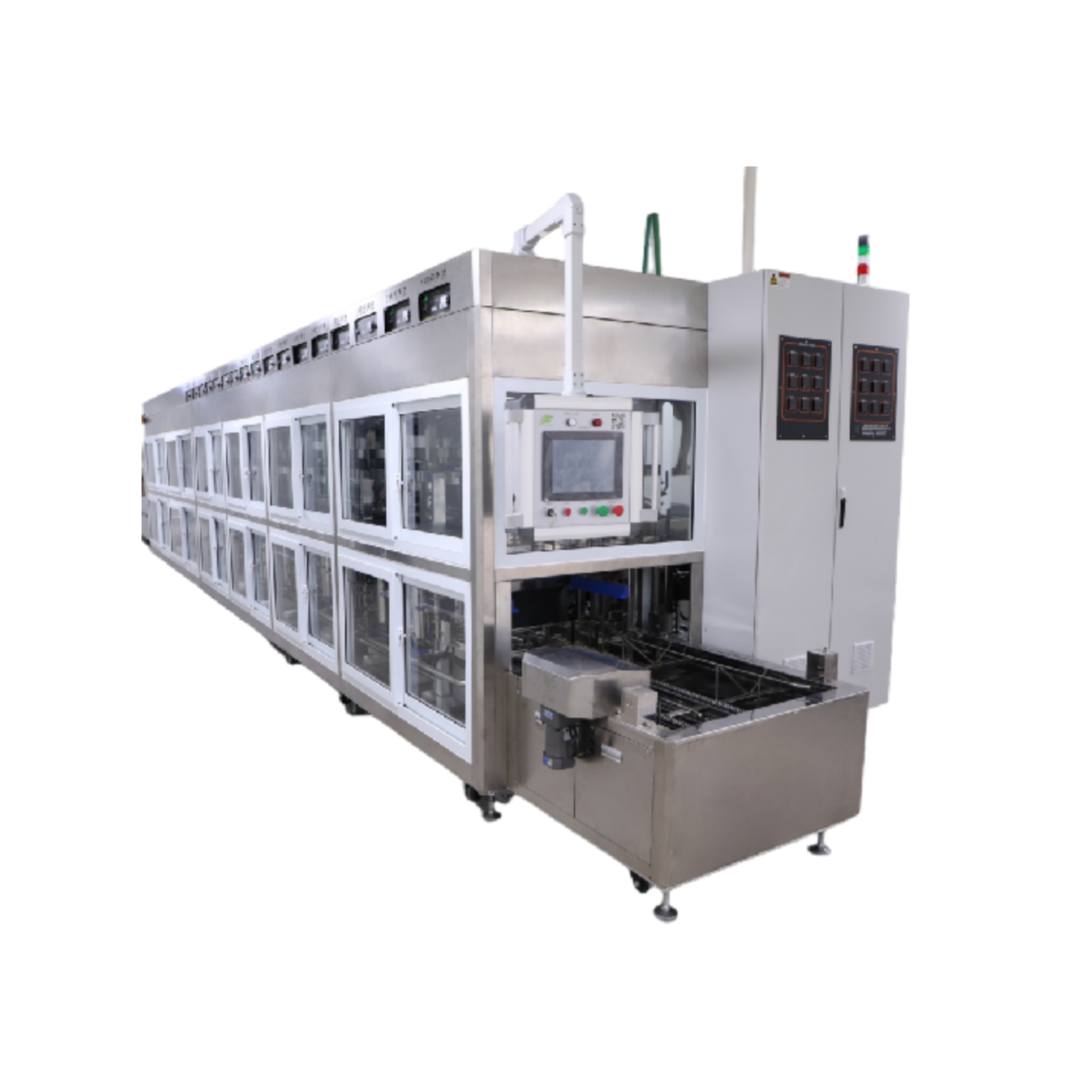
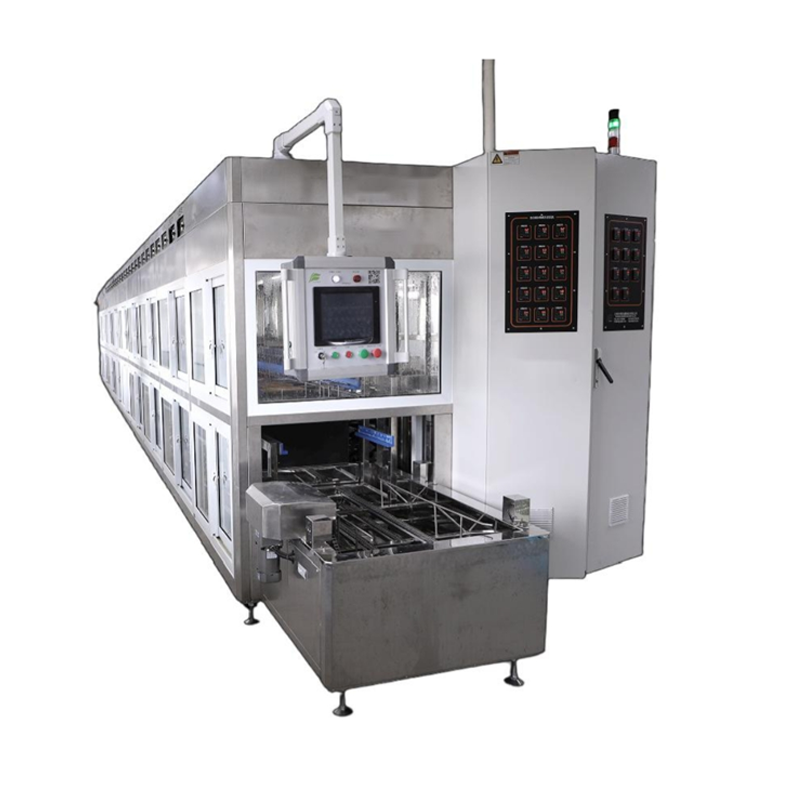
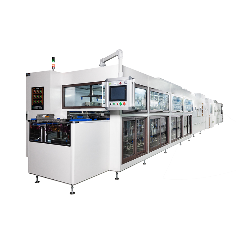
I. Product Description
Designed specifically for the semiconductor manufacturing process, it can be used for cleaning wafers, chips, semiconductor packages, photolithography masks, and semiconductor production process tools, etc. It can efficiently remove fine contaminants such as residual photoresist, metal particles, oil stains, and dust on the surface. Moreover, the cleaning process is non-contact, avoiding damage to the surface of precision components and ensuring the performance stability of semiconductor devices.
II. Working Principle
The equipment generates high-frequency electrical signals through an ultrasonic generator, which are then converted into high-frequency mechanical vibrations by a transducer and transmitted into the cleaning solution. Vibration forms countless tiny bubbles. During the growth and closure of these bubbles, a strong cavitation effect is generated, releasing a huge impact force that precisely acts on the surface of semiconductor components and tiny crevices, thereby stripping and removing contaminants. Some models are equipped with a sweep frequency function, which can ensure uniform sound field distribution and eliminate cleaning dead corners.
III. Core Advantages
1. Precise cleaning, non-destructive protection
Adopting multi-frequency adjustable ultrasonic technology ranging from 37kHz to 120kHz, combined with a swept-frequency sound field design, it ensures that the cleaning energy evenly covers the surface of the components and tiny crevices, leaving no cleaning dead corners. It supports three cleaning modes: "gentle/Standard/powerful". Sensitive chips, precision masks and other vulnerable components can be adapted to the low-power gentle mode to avoid surface scratches or performance damage. The removal rate of contaminants is as high as over 99.5%.
2. Intelligent and efficient, easy to operate
Equipped with a high-definition touch panel, it can visually set the cleaning time (adjustable from 3 to 30 minutes), temperature (precisely controlled from 20 to 80℃), and cleaning mode. Parameters can be saved with one click, and it supports quick invocation in batch cleaning scenarios. It is equipped with intelligent functions such as automatic heating, constant temperature triggering, and alarm upon completion of cleaning. It does not require manual supervision. The efficiency of single-batch cleaning is 5 to 8 times higher than that of traditional manual cleaning, significantly reducing labor costs.
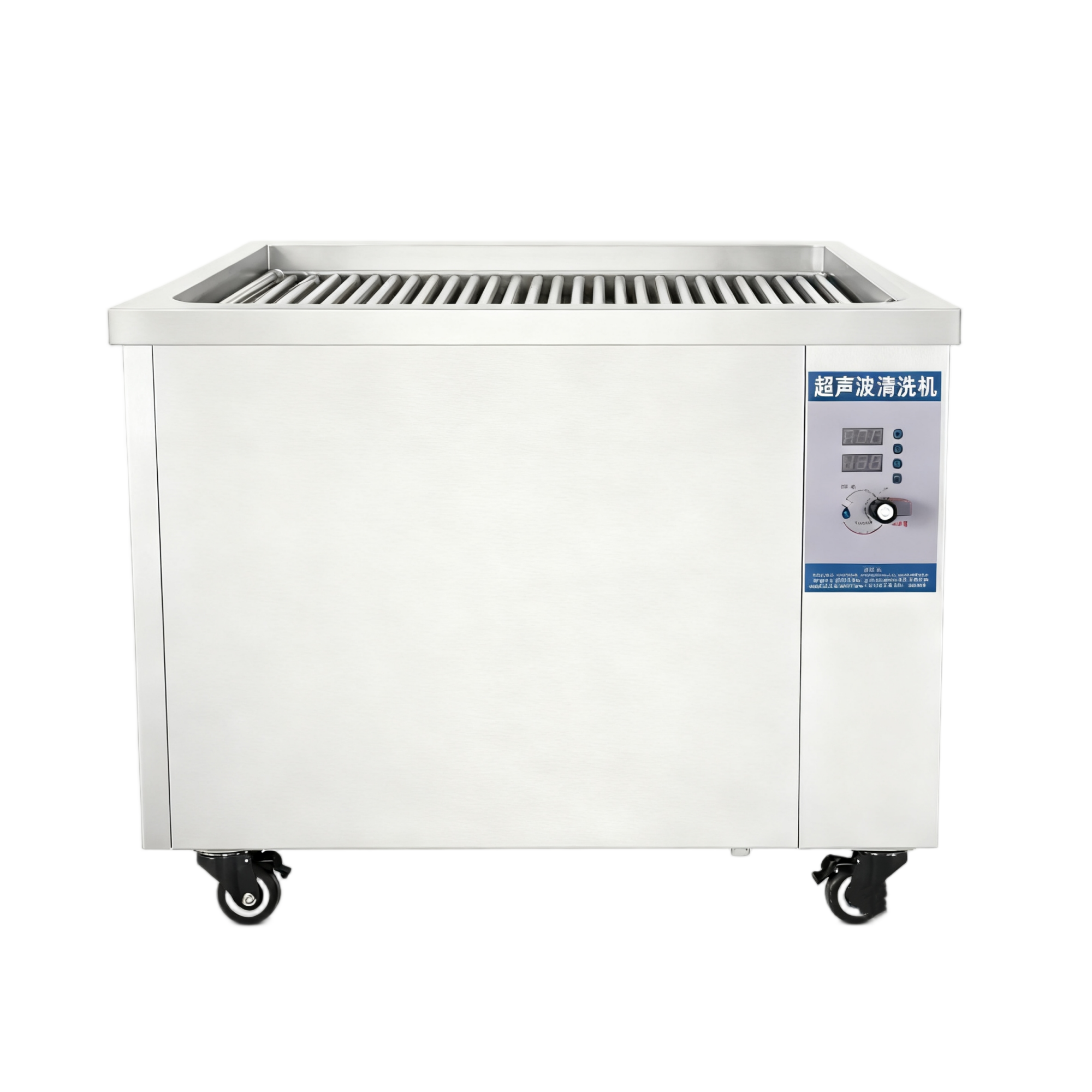
3. Stable and durable, safe and reliable
The inner tank is made of 304/316L corrosion-resistant stainless steel, which is resistant to acids, alkalis and aging, and is compatible with environmentally friendly cleaning agents specifically designed for semiconductors. The core transducer adopts an industrial-grade waterproof packaging design and has a service life of over 8,000 hours. It is equipped with multiple safety mechanisms such as anti-dry burning, anti-leakage, liquid level protection and overload protection. It complies with the ISO 9001 quality system and the safety standards of the semiconductor industry. The failure rate of the whole machine operation is less than 0.5%.
4. Flexible adaptation, diverse scenarios
The tank specifications cover capacities ranging from 5L to 100L, with inner tank sizes available from 300×135×150mm to 350×350×350mm, catering to various cleaning requirements such as single wafers, multi-chip batches, and large-scale process tools. Standard equipped with a dedicated stainless steel cleaning basket (with a load capacity of up to 5kg), it supports customized basket design to meet the precise positioning cleaning requirements of special-shaped components. Compatible with various cleaning media such as neutral cleaning agents and semiconductor-specific environmentally friendly solvents, it is suitable for different types of pollutant treatment scenarios.
IV. Applicable Scenarios
Semiconductor wafer manufacturing: Remove residual photoresist on the wafer surface, metal ion contamination, grinding dust, etc., to ensure the accuracy of photolithography and etching processes;
Chip packaging and testing: Clean the solder paste residue, pin oxide layer and contaminants on the surface of the test fixture before chip packaging to improve the packaging yield.
Maintenance of photolithography mask plates: Remove tiny particles and organic contaminants from the surface of the mask plate to prevent chip failures caused by mask defects.
Semiconductor process tools: Clean wafer carriers, quartz boats, reaction chamber components, etc., remove process residues, and extend the service life of tools.
V. Core Values
Technology empowerment: Multi-frequency ultrasonic waves combined with intelligent temperature control technology achieve the dual goals of "precise cleaning + non-destructive protection", meeting the high-precision requirements of semiconductor components.
Efficiency improvement: The fully automatic operation mode reduces manual intervention, and the batch cleaning capacity meets the rhythm of industrial production. The cleaning efficiency is increased by more than 50% compared with the traditional method.
Cost optimization: Extend the service life of semiconductor components and process tools, reduce the rate of defective products, and at the same time, the design of environmentally friendly cleaning agents is adapted to reduce the cost of pollution treatment.
Safety and Compliance: Complies with the clean standards and safety regulations of the semiconductor industry. Multiple protection mechanisms ensure the operation of equipment and the safety of operators, meeting the usage requirements of clean workshops.
This equipment can be designed, developed and manufactured according to different product specifications and production capacities.
 Slovenian
 Slovak
 Latvian
 Bosnian
 Icelandic
 Ukrainian
 Georgian
 Serbian
 Croatian
 Belarusian
 Romanian
 Estonian
 Hungarian
 Czech
Czech
 Catalan
 Norwegian
 Lithuanian
 Albanian
 Hindi
Hindi
 Italian
 Finnish
 Arabic
 Danish
 Bulgarian
 Thai
Thai
 Polish
 Swedish
 Greek
Greek
 Portuguese
 Dutch
Dutch
 Turkish
 Russian
 Deutsch
 French
 Korean
 Japanese
 English

Leave A Comment